
.png)
Zynq 7020 SoC Development Board (Micro-Zynq7)
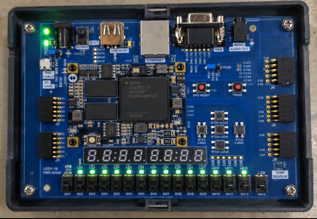
Zynq 7020 SoC Development Board (Micro-Zynq7)
This FPGA Dev Board is a powerful, versatile real time control prototyping System. Coupled with an easy and powerful MATLAB-SIMULINK model- based development environment, push button device, 20x4 LCD Display, Powerful Application software, it forms a complete control prototyping solution. It provides an embedded processing system (PS) with tightly integrated programmable logic and a rich set of configurable I/O capabilities.
Based on Dual core A9 Processor with logical Cells, DSP Slices and many on board features. This Zynq 7020 FPGA Development Board is an ideal solution for FPGA Components and its interface with real world like switches, ADC, DAC, Display etc.
ZYNQ SoC FPGA Development Board is a feature rich and high-performance Single Board Computer built around the Xilinx Zynq Z7020 FPGA. It features integrated dual-core ARM Cortex-A9 processor with Xilinx 7-series FPGA. ZYNQ SoC FPGA Development Board is designed to create best learning experience of both processing system (PS) and programming logic (PL). It also features 512MB DDR3 SDRAM and 16MB QSPI Flash USB-to-UART, USB OTG, 10/100/1000Mbps Ethernet, HDMI, USB JTAG, Temperature sensor, Micro SD, Wi-Fi, Bluetooth, ADC, LCD, 7 Segment, Camera, TFT, Buzzer, Switches, buttons and LEDs.
- Core architecture - Zynq 7010 : 33,280 Logic Elements, 400 Distributed Memory RAM, 90 DSP48E1 Slices - Zynq 7020 : 52,160 Logic Elements, 600 Distributed Memory RAM, 120 DSP48E1 Slices
- ZYNQ XC7Z020-1CLG400C
- 650MHz dual-core Cortex-A9 processor
- DDR3 memory controller with 8 DMA channels
- High-bandwidth peripheral controllers: 1G Ethernet, USB 2.0, SDIO
- Low-bandwidth peripheral controller: SPI, UART, CAN, I2C
- Programmable from JTAG, Quad-SPI flash, and microSD card
- Programmable logic equivalent to Artix-7 FPGA
- 13,300 logic slices, each with four 6-input LUTs and 8 flip-flops
- 630 KB of fast block RAM
- Based on AMD Xilinx Zynq 7010/7020 Device.
- SDRAM: 32MB(256Mbit) SDRAM
- SPI FLASH : 64 Mb FLASH for XC7A35T FPGA Configuration
- SPI FLASH : 128 Mb FLASH for XC7A100T FPGA Configuration
- Complete suite of DSP IPs for Algorithmic Acceleration.
- Up to 15 dedicated clock pins that can drive up to 10 global clocks Phase-locked loops (PLLs)
- Up to four general purpose PLLs
- Software Support: Compatible with Vivado Software and supports development using Verilog, VHDL, C/C++ and Python.
- 16nos of SPDT switch for Input purpose
- 16nos of LED for Output purpose
- 16X2 LCD
- 4nos 7-segment LED display
- 1no of Buzzer
- ADC : 4 Channel XADC input with 3.3v input compatible
- 2Ch ADC, 12bit, 200KSPS terminated at Screw Type Connector
- 2Ch DAC, 12bit, 8.5uS Settling Time, terminated at Screw Type Connector
- 4 Push Button Switches
- 16 External I/O terminated at 20 Pin Connector.
- Wi-Fi & Blue Tooth : ESP32 WiFi
- VGA : 12-bit, 4096 Color
- HDMI : HDMI OUT
- Sensor1 : LM35 Temperature Sensor
- Sensor2 : LDR
- Sensor3 : Accelerometer
- MicroSD Card
- USB JTAG for Programming and Debugging. Fully Compatible with Xilinx Vivado Tool
- USB UART with programmable baud rate
- Programming : Compatible with Xilinx Vivado Tool. Vivado provides the complete programme development environment required to create an FPGA project, write HDL code, assign FPGA pins, compile the design, check timing and resource usage, generate the programming file, and download the design into the FPGA through the JTAG interface.
- Applications : Ideal for Embedded Systems, Digital Signal Processing (DSP), Image and Video Processing, Robotics, IoT, and FPGA-based research and education.